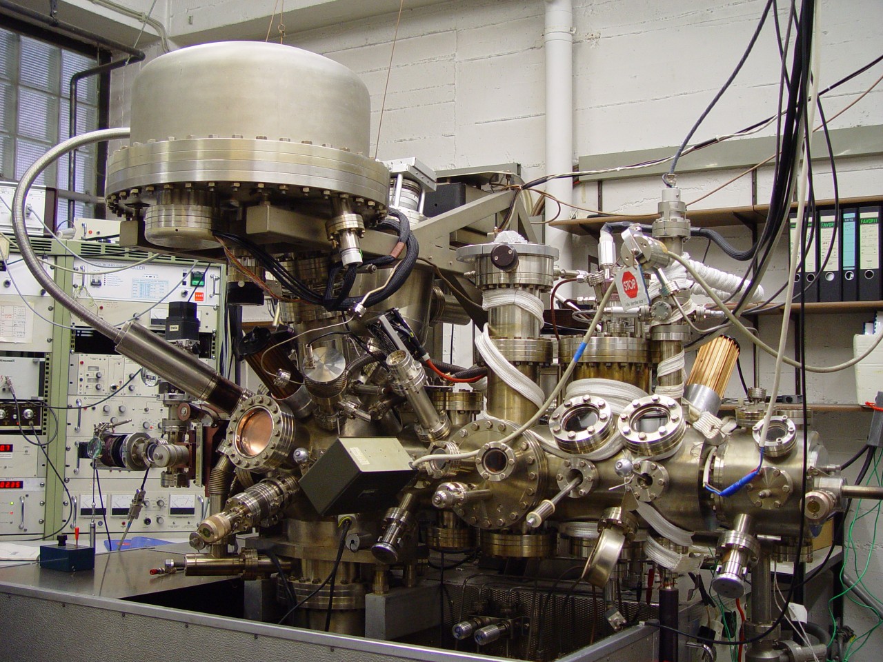
Photoelectron spectrometer, ESCALAB Mk II by Vacuum Generators
Analysis:
- X-Ray Photoelectron Spectroscopy (XPS)
- X-Ray Photoelectron Diffraction (XPD)
- Electron Energy Loss Spectroscopy (EELS)
- Low Energy Electron Diffraction (LEED)
- Ultraviolet Photoelectron Spectroscopy (UPS)
- Angle Resolved Ultraviolet Spectroscopy (ARUPS)
- Fermi-Surface Mapping (FSM)
- Mass Spectrometry (MS)
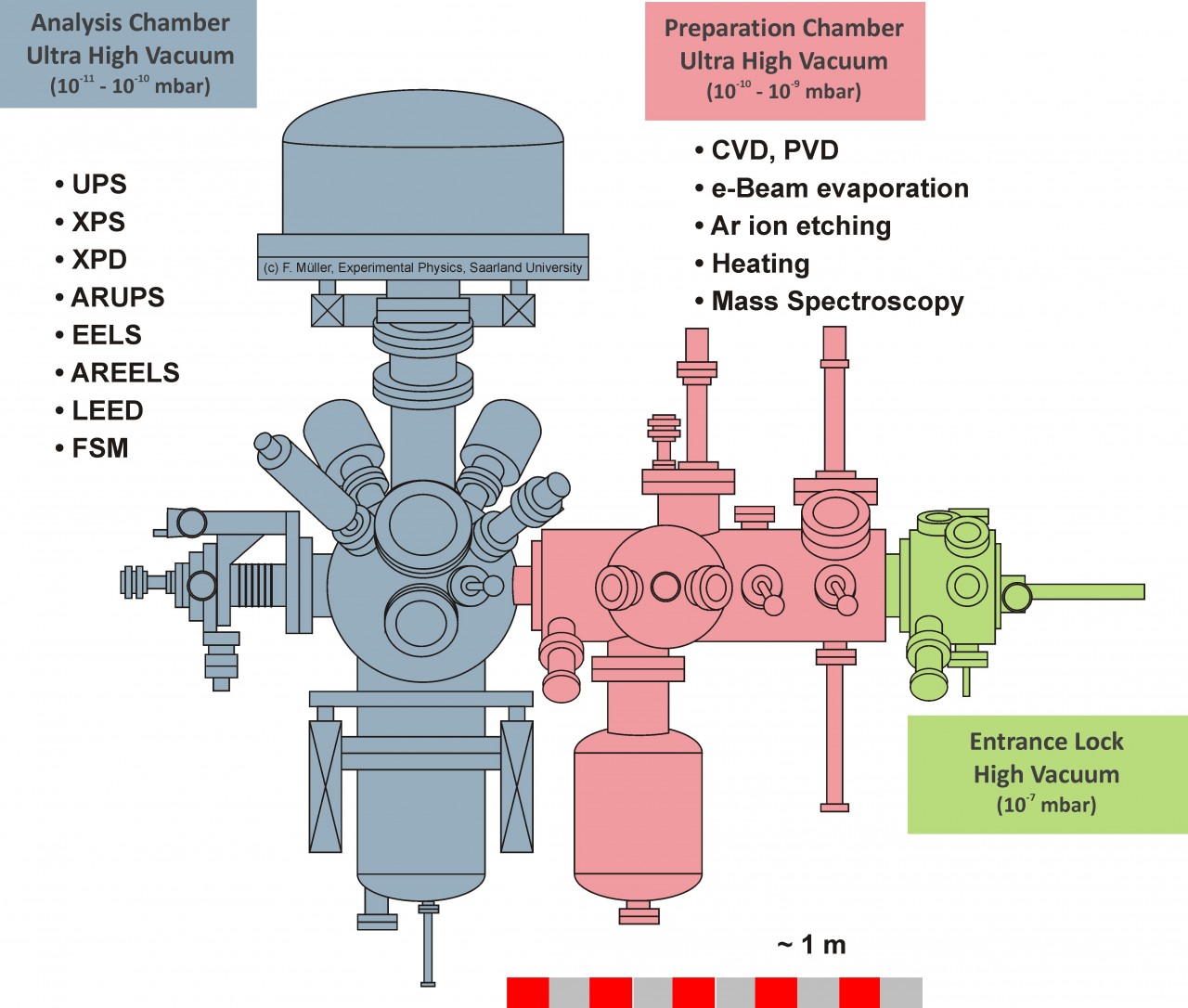
Synthesis:
- Electron Beam Evaporation
- Several heating stages (up to ca. 1000 K)
- Ar ion etching
- Chemical Vapor Deposition (CVD)
Sample specifications:
- Area: typically ca. 10 mm x 10 mm, thickness: ca. 1-2 mm
X-Ray Photoelectron Spectroscopy
XPS provides an experimental standard tool for surface analysis. XPS excels by its very high surface sensitivity, i.e., due to the very small electron mean free paths of electrons with kinetic energies in the range of 10–2000 eV (typically 1-2 nm) only the topmost layers of a sample are probed. Photoelectrons are detected in terms of their distribution of kinetic energies (as a measure of their binding energy) and their distribution of momentum with respect to, e.g., the crystal axes of the sample.
The distribution of binding energies provides information on the chemical composition of the sample, since binding energies are a characteristic fingerprints for each element. The distribution of intensities provides information on the stoichiometry of the sample. Furthermore, for atoms bonded in different “chemical environment”, the so-called chemical shift of binding energies provides information of the electronic state of this atom (i.e., X0, X-1, X+2, etc.). Therefore, XPS was originally established as Electron Spectroscopy for Chemical Analysis (ESCA).
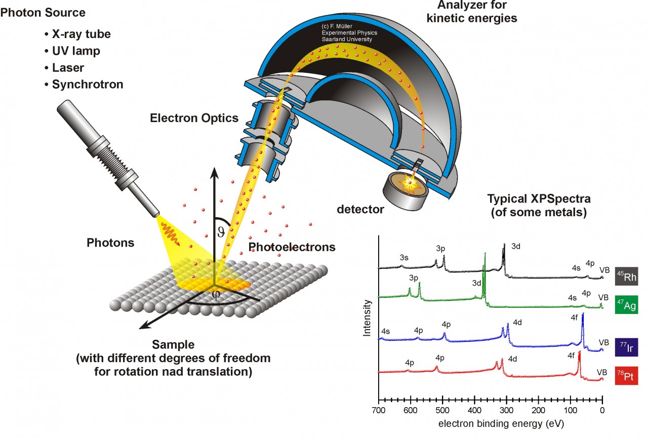
Schematic drawing of a typical XPS setup with photon source (X-rays, UV-light, laser or Synchrotron radiation), a sample manipulation with different linear and rotational degrees of freedom, electron optics, an energy dispersive analyzer and a detector. XP spectra (intensity vs. binding energy) are shown for four different metals with their element specific distribution of core level photoemission.
In the fields of polymer film formation, flow properties of complex fluids as well as adhesion of biomaterials, silicon wafers with native or extended oxide layers (thickness ca. 2 nm or 150 nm) are often used as model surfaces. It is known, that the surface properties are determined by the topography as well as by the chemistry of the surface. In the latter case, it is also the chemistry of the sub-surface region of the sample that has a distinct impact on bonding interactions, such as, e.g., long range Van der Waals forces. Therefore, a detailed knowledge of the chemistry of the uppermost layers is necessary to reveal the wetting or adhesion properties of a particular surface. Due to its high surface sensitivity, XPS provides an ideal tool to explore the chemical nature of a sample layer-by-layer when combined with Ar ion etching.
For example, the native oxide of a silicon wafer consists of a mixture of Si4+, Si3+, Si2+ and Si1+. Are these valencies mixed throughout the whole oxide layer or is there a kind of stacking of different valencies? XPS depth profiling experiments give evidence that the latter scenario is valid. The topmost ~1 nm is formed by SiO2 whereas the ~1 nm interface layer is formed by the Si3+, Si2+ and Si1+ valencies.
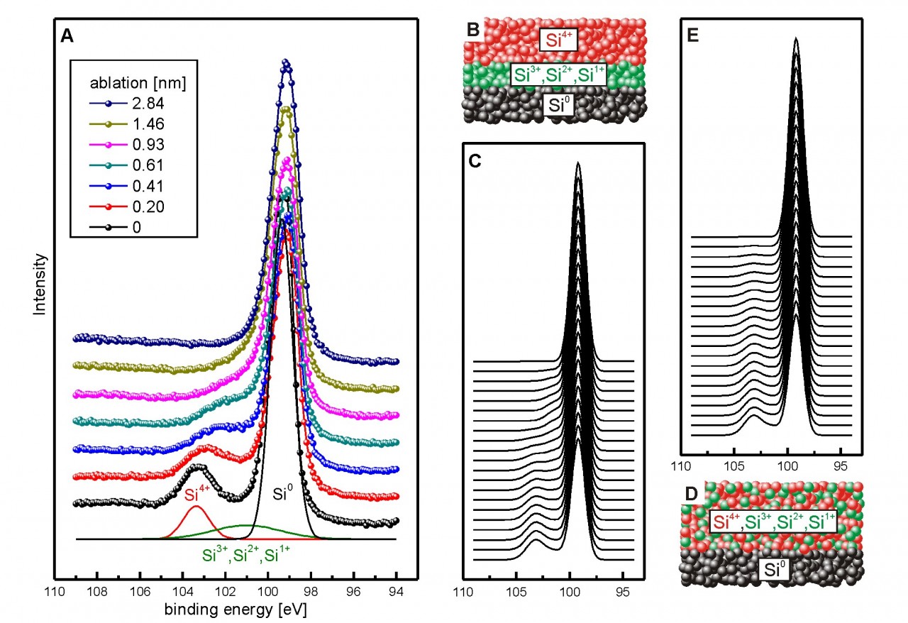
(A) XPS data of a silicon wafer with native oxide layer in the range oft he Si-2p photoemission for different steps of ablation. The spectrum is approximated by the main Si0-peak, a Si4+ peak and a broad peak containing contributions from Si3+, Si2+ and Si1+. With increasing depth (ablation), the intensity of the Si4+-peak decreases and shifts towards the main Si0-peak.
(B) Surface model of stacked oxide layers Si4+ - Si3+, Si2+, Si1+ - Si0.
(C) Calculated spectral shapes for the model in (B). The Si4+-peak decreases and shifts towards the main Si0-peak as observed in the experimental data.
(D) Surface model of mixed oxide layers Si4+, Si3+, Si2+, Si1+ - Si0.
(E) Calculated spectral shapes for the model in (D). The Si4+-peak just decreases without shifting towards the main Si0-peak.
Figure according to P. Loskill et al., Adv. Coll. Interf. Sci. 107 (2012) 179182.
 Deutsche Version